|
Differential Amplifier DC Analysis
by
Robert L Rauck
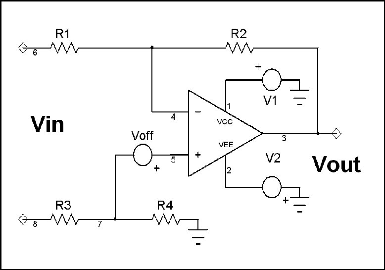
Amplifier DC performance is affected by a variety of Op Amp characteristics. Not all of these factors are commonly well understood. This analysis will develop complete expressions for analyzing the DC performance of an differential amplifier including the effect of bias current, offset current and offset voltage. Accurate assessment of performance over a wide range of conditions will then be possible. The two amplifier input terminal currents will be labeled Iminus and Iplus . Most bipolar Op Amps (but not all) have input stages arranged such that current flows into the amplifier input pins. The situation is more complex with FET input devices where the dominant input current term is a leakage current.
|
Eq. 1
|
Iminus will be defined as positive when it flows into the Op Amp negative input terminal.
|
|
Eq. 2
|
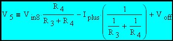
Iplus will be defined as positive when it flows into the Op Amp positive input terminal. The positive end of Voff is indicated in the diagram
|
|
Eq. 3
|
G is the open loop gain of the Op Amp and can be broken down further into a DC term multiplied by an expression accounting for gain changes with frequency.
|
|
|
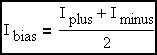
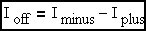
We will define offset current to be positive when it results from a current (Ioff/2) that flows into the Op Amp negative input terminal and out of the positive input terminal.
|
|
Therefore
|
|
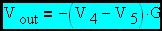
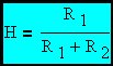
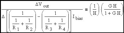
H is (by definition) the gain from Vout to V4 with all other voltage sources shorted and all current sources open (Op Amp loading of V4 ignored). This is part of the analysis by the very powerful superposition process.
|
|
Eq. 4
|
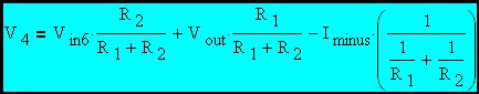
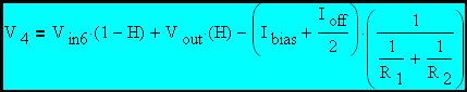
Effective voltage at the Op Amp inverting input after the substitution of expressions involving H, Ibias and Ioff.
|
|
Eq. 5
|
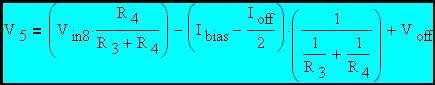
Effective voltage at the Op Amp non-inverting input after the substitution of expressions involving Ibias and Ioff.
|

|
Substituting EQ. 4 and EQ. 5 into EQ. 3
|

|
Collecting terms involving Ibias and Ioff.
|

|
Collecting terms involving Vout.
|
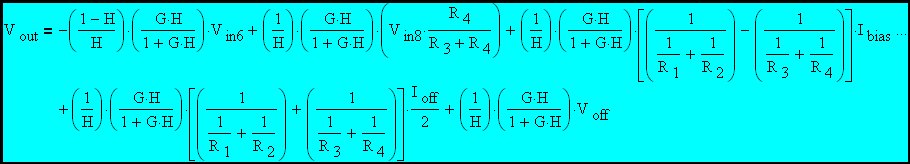
Next we will rearrange the expression so that the right-hand side is a summation of expressions that involve each of the signals applied to the amplifier. This is one step closer to the desired final form of the gain equation.
|
|
Eq. 6
|
Let us now resolve the two input voltages into common mode and differential mode components:
|
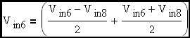
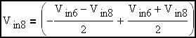
One half of the differential mode input voltage plus the common mode input voltage
|
|
Minus one half of the differential mode input voltage plus the common mode input voltage
|
Now let's substitute these terms into EQ. 6:
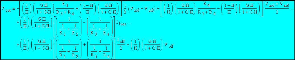
Now let's collect terms associated with the common mode input voltage and those associated with the differential mode input voltage. This will put the expression in a particular version of standard form that is a very low entropy expression that brings out the relationships that drive performance.
|
|
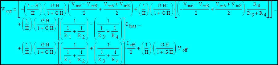
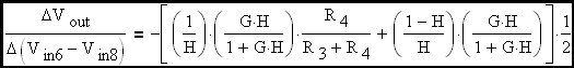
Eq. 7
|
Examination of this last expression reveals that the output is again expressed as the sum of several terms. The first of these terms is a function of the actual desired differential input signal, the second is a function of the common mode input signal and the rest are functions of undesired, but very real, parasitic inputs (input voltages and currents that are generated by the Op Amp). Each of the effective inputs (except the actual intended differential input signal and the common mode input signal) has been arranged so that the gain expression is recognized as being in the standard non-inverting format.
Further examination of this expression reveals that each term on the right is composed of an expression that assumes infinite Op Amp gain times a correction term (G*H/(1+G*H)) that accounts for Op Amp gain effects. The two terms involving currents also include an equivalent resistance to convert the current to a voltage. Closer examination of these resistance terms reveals that the coefficient of Ibias is the difference between two resistances while the coefficient of Ioff is the sum of these two resistance terms. The term involving R1 and R2 is the parallel combination of these two resistances and the term involving R3 and R is the parallel combination of these two resistances. One can quickly recognize these terms as the Thevenin equivalent resistance attached to the two Op Amp inputs. An excellent thing happens when the two Thevenin equivalent impedances are set equal to each other. The term involving Ibias is now multiplied by zero and disappears. Then the error term involving the currents is reduced to one involving only Ioff which is usually much smaller than Ibias. This explains the reason for matching the impedances at the two Op Amp inputs. Designers also frequently try to match the AC impedances (at the amplifier inputs) across frequency although the benefit gets much smaller very quickly as the amplifier gain decreases and the differential input current grows.
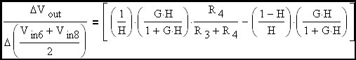
Taking the derivatives of the left hand side of EQ. 7 with respect to the individual input signals reveals the corresponding gain terms:
|
Here the differential gain is one half the sum of the gains associated with thew two individual input signals.
|
|
Eq. 8
|
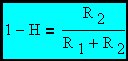
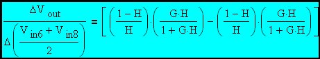
If R4/(R3+R4) is set equal to R2/(R1+R2) = 1-H then this simplified expression results. This is the classic inverting amplifier gain expression.
|
|
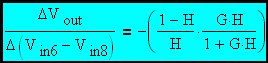
Here the common mode gain is the difference between the gains associated with the two individual input signals.
|
|
Eq. 9
|
If R4/(R3+R4) is set equal to R2/(R1+R2) = 1-H then the right hand side of this expression equals zero and the common mode component of input voltage is completely rejected at the output. Complete cancellation is impossible but very good attenuation is possible in most cases.
|
|
The classic non-inverting amplifier gain expression. The other two gain terms will have this same form on the right-hand side of the equals sign.
|
This analysis has developed a complete expression for the DC gain of the differential amplifier including the effects of Amplifier Gain, Ibias, Ioff and Voff. This expression can now be used to predict output voltage stability. For example, if the loop gain is 1,000 then G*H/(1+G*H)=1,000/1,001~0.999 so the ideal gain is degraded by 0.1% error due to low loop gain. A typical Op Amp has a DC gain that is very high so H would have to be a very small number (big attenuator) to cause this much gain error. In a similar fashion, output voltage error terms can be computed for Ibias, Ioff and Voff. Amplifier specifications provide expected variations in all these parameters over temperature so the effect of these variations can easily determined. The expression for G*H does not include the DC signal inversion (internal to the Op Amp) represented by the inverting input pin. Therefore the value of G is a positive number at DC in spite of the minus sign on the inverting input pin. This signal inversion is accounted for by the minus sign just after the equals sign in EQ. 8.
It should be noted that amplifier input and output voltages must remain within their specified linear ranges for the above analysis to hold. Most amplifiers do not allow rail-to-rail operation of input and output voltages. It should also be noted that Op Amps have a specified minimum input impedance (common mode and differential mode). This means that Op Amp input currents are more complex than simple current sources and will be somewhat affected by input voltage variations. An even more accurate model would result if these impedances were included in the gain expression. This effect becomes more important as the impedances external to the Op Amp become larger and does not significantly affect many applications.
Differential amplifiers also are subject to a (potentially significant) source of error that is not always obvious to the designer. The differential input signal is frequently small compared to the common mode input signal. The amplifier is then faced with the need to extract the small difference between two large numbers and amplify it accurately. Any mismatch between the resistance networks at the two inputs to the amplifier will prevent complete cancellation of the common mode term (EQ. 9) and proper extraction of the differential mode term. Remember a 1% error in the two common mode gain terms will lead to an error term as large as the desired signal if the common mode voltage is 100 times as large as the differential mode voltage. In some cases the designer can make changes to minimize the ratio of common mode to differential mode voltage and this is highly desirable if it does not cause other problems. For this reason, use the complete expression (EQ. 7) rather than the simplified expresions and carefully analyze the result of worst case component value mismatches (include temperature and aging effects). This situation also makes these amplifiers sensitive to conducted and radiated noise especially at higher frequencies.
|